
Semiconductor Devices
Class 12 Physics Notes • NEB Syllabus 2083
Syllabus, 10 solved multiple choice questions, step-by-step answers with diagrams and truth tables, handwritten and typed PDF notes and frequently asked questions on the p-n junction, diodes, full-wave rectification and logic gates.
1. Syllabus
Unit: Modern Physics
Chapter 22: Semiconductor Devices (6 hours)
These notes follow the NEB Class 12 Physics syllabus (+2 Physics, Nepal). Practise the multiple choice questions first, then work through the numericals, and finish with the PDF notes for quick revision.
2. Multiple Choice Questions
Question 1. Barrier potential difference is the potential difference across:
- a) terminals of a cell
- b) depletion layer of a p-n junction
- c) capacitor plates
- d) ends of a conductor
Correct Answer: b) depletion layer of a p-n junction
Reason: Electrons diffuse from the n-side to the p-side and holes from the p-side to the n-side. This leaves uncompensated positive donor ions on the n-side and negative acceptor ions on the p-side. This region is the depletion layer, and the potential difference set up across it by these fixed ions is the barrier potential difference.
Question 2. The current through a p-n junction is negligible when the junction is:
- a) forward biased
- b) reverse biased
- c) positive biased
- d) negative biased
Correct Answer: b) reverse biased
Reason: In reverse bias the applied voltage widens the depletion layer and raises the barrier, so majority carriers cannot cross. Only a very small leakage current of thermally generated minority carriers flows.
Question 3. A reverse biased p-n junction has:
- a) very narrow depletion layer
- b) almost no current
- c) very low resistance
- d) large current flow
Correct Answer: b) almost no current
Reason: Reverse bias widens the depletion layer and increases the potential barrier. The junction then has very high resistance and only a tiny reverse saturation current flows, so there is almost no current.
Question 4. Which device is used to convert alternating current into direct current?
- a) transformer
- b) rectifier
- c) diode
- d) triode
Correct Answer: b) rectifier
Reason: A rectifier is the device (circuit) that converts alternating current, which reverses direction periodically, into direct current, which flows in one direction only. Diodes are the components from which a rectifier is built.
Question 5. A Zener diode can be used as a:
- a) rectifier
- b) voltage regulator
- c) oscillator
- d) voltage divider
Correct Answer: b) voltage regulator
Reason: A Zener diode works in its reverse breakdown region, where the voltage across it stays almost constant while the current changes widely. Connected in parallel with the load, it keeps the output voltage nearly constant, so it acts as a voltage regulator.
Question 6. All logic gates can be made by the repetitive use of:
- a) OR gates
- b) AND gates
- c) NOT gates
- d) NAND gates
Correct Answer: d) NAND gates
Reason: NAND (and NOR) gates are called universal gates: any basic gate (AND, OR, NOT) or any Boolean expression can be built using only NAND gates.
Question 7. What is the minimum number of NAND gates required to implement a NOT gate?
- a) 1
- b) 2
- c) 3
- d) 0
Correct Answer: a) 1
Reason: Join the two inputs of a NAND gate together and apply \(A\) to both. The output is
which is the NOT operation. Only one NAND gate is needed.
Question 8. Which of the following is given by this logic circuit? (Input A goes to both inputs of one NAND gate, input B goes to both inputs of a second NAND gate, and the outputs of these two gates are the inputs of a third NAND gate.)
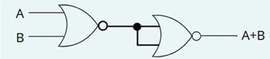
Figure for Question 8
- a) OR gate
- b) AND gate
- c) NAND gate
- d) NOT gate
Correct Answer: a) OR gate
Reason: The first gate gives \(\overline{A\cdot A}=\overline A\) and the second gives \(\overline B\). The third gate gives
using De Morgan’s law. \(A+B\) is the output of an OR gate.
Question 9. Which of the following is given by this logic circuit? (Inputs A and B go into an OR gate, and the output of the OR gate goes into a NOT gate.)
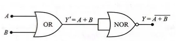
Figure for Question 9
- a) OR gate
- b) AND gate
- c) NAND gate
- d) NOR gate
Correct Answer: d) NOR gate
Reason: The OR gate gives \(A+B\) and the NOT gate inverts it, so \(Y=\overline{A+B}\). An OR gate followed by a NOT gate is a NOR (NOT-OR) gate.
Question 10. Boolean algebra is essentially based on:
- a) logic
- b) truth
- c) number
- d) symbol
Correct Answer: a) logic
Reason: Boolean algebra is the algebra of the truth values true and false (written 1 and 0). It is used to analyse and simplify logical statements and digital circuits, so it is essentially based on logic.
3. Numerical and Subjective Questions
a) Explain the formation of the potential barrier and the depletion layer in a p-n junction.
When a p-type and an n-type semiconductor are joined, there is a concentration gradient: the p-region has a high concentration of holes (majority carriers) and the n-region has a high concentration of free electrons.
Because of this gradient, electrons diffuse from the n-side into the p-side and holes diffuse from the p-side into the n-side. An electron leaving the n-side leaves behind a fixed positive donor ion. An electron entering the p-side recombines with a hole and creates a fixed negative acceptor ion.
Near the junction there is therefore a region containing only immobile positive and negative ions, with no mobile charge carriers. This region is the depletion layer.
The positive ions on the n-side and the negative ions on the p-side set up an electric field directed from the n-side to the p-side. This field produces a potential difference across the junction, the barrier potential (or potential barrier) \(V_0\), which opposes the further diffusion of majority carriers. Equilibrium is reached when the drift current due to the field balances the diffusion current.
Figure: Depletion layer and barrier potential of a p-n junction
b) Explain the forward and reverse characteristics of a p-n junction diode.
Forward bias. The positive terminal of the battery is connected to the p-type and the negative terminal to the n-type material. The applied voltage opposes the barrier potential, so the barrier becomes lower and the depletion layer narrower. Majority carriers can then cross the junction. Once the applied voltage exceeds the cut-in (knee) voltage (about 0.7 V for silicon), the current increases rapidly (exponentially) with the voltage. The diode has very low resistance in this state.
Reverse bias. The negative terminal is connected to the p-type and the positive terminal to the n-type material. The applied voltage adds to the barrier potential, so the depletion layer widens and the barrier increases. The flow of majority carriers almost stops. The strong field sweeps thermally generated minority carriers across the junction, giving a very small, nearly constant current called the reverse saturation current. If the reverse voltage is increased beyond the breakdown voltage, the reverse current suddenly increases greatly (avalanche or Zener breakdown), and an ordinary diode can be destroyed by the heat.
Figure: V–I characteristic of a p-n junction diode
a) What is a junction diode? Explain a full-wave rectifier using two diodes.
A junction diode is a semiconductor device formed by joining a p-type and an n-type semiconductor. It conducts easily in forward bias and blocks the current in reverse bias.
Full-wave rectifier. It converts the whole of the input alternating cycle into pulsating direct current. It uses a centre-tapped transformer and two diodes \(D_1\) and \(D_2\). The ends of the secondary coil are connected to the p-sides of the two diodes, the n-sides are joined together and connected to the load resistor \(R_L\), and the other end of \(R_L\) is connected to the centre tap.
Figure: Full-wave rectifier using two diodes
Working. In the positive half cycle the upper end of the secondary is positive with respect to the centre tap, so \(D_1\) is forward biased and conducts through \(R_L\), while \(D_2\) is reverse biased. In the negative half cycle the polarity reverses, \(D_2\) conducts and \(D_1\) is cut off. In both half cycles the current passes through \(R_L\) in the same direction, so the output across the load is unidirectional (pulsating direct current).
b) What will happen if one of the diodes is damaged?
If one diode (say \(D_2\)) becomes an open circuit, the rectifier works only in the half cycle in which the other diode is forward biased. It becomes a half-wave rectifier: the output exists for only half of each cycle, the ripple increases and the average output voltage and efficiency fall.
c) The output of a full-wave rectifier is pulsating direct current. Which device can be used to get a constant output voltage? Draw its symbol and its characteristics.
A Zener diode is used as a voltage regulator. It is connected in reverse bias, in parallel with the load, usually after a filter capacitor.
Figure: Symbol and characteristic of a Zener diode
In the forward region the characteristic is like that of an ordinary diode. In the reverse region, when the reverse voltage reaches the Zener breakdown voltage \(V_Z\), the current rises sharply, and the voltage across the diode stays almost constant at \(V_Z\) over a wide range of current. Therefore the output voltage across the load is held at \(V_Z\).
a) What are logic gates? Give the truth table for a two-input NAND gate with its symbol.
Logic gates are the basic building blocks of digital electronic circuits. They perform logical operations based on Boolean algebra: they take one or more binary inputs (0 or 1) and give one binary output according to a logical rule.
Figure: Symbol of a NAND gate
The NAND gate is “NOT AND”. Its output is 0 only when both inputs are 1; otherwise the output is 1: \(Y=\overline{A\cdot B}\).
| A | B | Y = (A·B)′ |
|---|---|---|
| 0 | 0 | 1 |
| 0 | 1 | 1 |
| 1 | 0 | 1 |
| 1 | 1 | 0 |
b) Explain why a NAND gate is considered a universal gate.
A NAND gate is a universal gate because the basic gates NOT, AND and OR can all be built using only NAND gates, so any digital circuit can be made from NAND gates alone.
Making circuits from many identical gates is also cheaper and easier in integrated-circuit manufacture.
a) Draw a circuit diagram to realise an AND gate from a NOR gate, with its truth table.
Use the De Morgan law: \(A\cdot B=\overline{\overline A+\overline B}\). So the inputs must be inverted and then fed into a NOR gate. A NOR gate becomes a NOT gate when its two inputs are tied together.
Figure: AND gate from three NOR gates
| A | B | A′ (NOR 1) | B′ (NOR 2) | Y = (A′ + B′)′ (NOR 3) |
|---|---|---|---|---|
| 0 | 0 | 1 | 1 | 0 |
| 0 | 1 | 1 | 0 | 0 |
| 1 | 0 | 0 | 1 | 0 |
| 1 | 1 | 0 | 0 | 1 |
b) Which gate will you get if you connect a NOT gate at the output of the circuit of part (a)?
The circuit of part (a) is an AND gate. A NOT gate at its output inverts the result, and an inverted AND gate is a NAND gate.
c) Show that the circuit given below acts as an OR gate using a truth table.
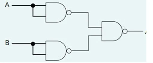
Figure for Question 4
Input A passes through a NOT gate to give \(\overline A\), and input B passes through a NOT gate to give \(\overline B\). These two signals enter a NAND gate:
| A | B | A′ | B′ | Y = (A′·B′)′ | A + B |
|---|---|---|---|---|---|
| 0 | 0 | 1 | 1 | 0 | 0 |
| 0 | 1 | 1 | 0 | 1 | 1 |
| 1 | 0 | 0 | 1 | 1 | 1 |
| 1 | 1 | 0 | 0 | 1 | 1 |
The output column of the circuit is the same as the column of \(A+B\), so the circuit acts as an OR gate.
4. View PDF Notes
i. Handwritten Notes
ii. Typed PDF Notes
5. Frequently Asked Questions
What is a semiconductor? (definition in physics)
What topics are included in Chapter 22 Semiconductor Devices of NEB Class 12 Physics?
What are the types of semiconductors?
What are examples of semiconductors?
What is a p-n junction and how is the depletion layer formed?
What is the semiconductor diagram of a p-n junction?
What are forward bias and reverse bias?
What is a rectifier and how does a full-wave rectifier work?
What happens if one diode of a full-wave rectifier is damaged?
What is a Zener diode and what is it used for?
What are logic gates?
What are the Boolean expressions of the NOT, OR, AND, NAND and NOR gates?
Why are NAND and NOR called universal gates?
What is a semiconductor chip and what are semiconductor companies and the semiconductor industry?
Where can I get Class 12 Physics Chapter 22 Semiconductor Devices notes in PDF?
Students also search for: